
Researchers
研究者名
Kaneko, Mitsuaki
研究者名
Mikami, Kyota
研究者名
Kimoto, Tsunenobu
Overview
Kyoto, Japan -- While silicon carbide -- SiC -- has long been promoted as the key to developing electronics suitable for extreme environments, the field has been stuck in the lab for some time. Now, a team of researchers focusing on junction field-effect transistors, or JFETs, have succeeded in developing a new SiC transistor structure that can operate at 600°C, as announced recently by Kyoto University.* One of the team's goals after their previous study was to scale up to wafer-level production, so that is what they have now accomplished.
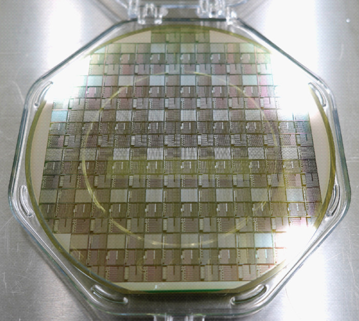
Compared with the previous study, wafer-scale production refers to building much smaller components and involves developing a minuscule but more efficient SiC transistor. Progressing to the wafer-scale is essential for practical implementation, as the fabrication of integrated circuits requires a large number of very small transistors.
However, wafer-scale production is virtually impossible to accomplish in a university laboratory due to equipment constraints. This motivated the team to collaborate with Phenitec Semiconductor Corp, which operates a mass-production fabrication plant, making this next step in their research feasible.
The team applied much of the same JFET fabrication process they had developed at the chip scale directly to the wafer scale, including an awareness of manufacturability in a mass-production plant at industry standards. This process was transferred without major obstacles.
The result was a SiC transistor, produced on a 6-inch wafer, that demonstrated high uniformity, with a threshold voltage standard deviation of less than 0.07 volts within the wafer center region. This is a technical milestone enabling the fabrication of integrated circuits.
"While we had expected the wafer-scale device fabrication itself to succeed, we were surprised that the uniformity in the wafer center region was this effective, even in the first fabrication trial," says first author Mitsuaki Kaneko.
This study represents a major step along the path towards the development of integrated circuit technology suitable for extreme environments. The combination of this progression to wafer-scale production and the team's recent research expand the application range of semiconductors.
This could open the door to application areas for electronic circuits that have so far not been accessible, such as jet engine sensors, geothermal resource development, and even the exploration of Venus.
"Between creating something in the laboratory and having it actually being used in society, there is a much larger gap than most people imagine," says Kaneko. "Through this industry-academia collaboration we are aiming to establish a startup, and though there remain many challenges, we will steadily work our way through them."
*See "A transistor that operates at 600°C", 24 August 2026