Working with ALS Technology Co Ltd (Sagamihara City, Kanagawa, Japan), Assistant Professor Hiroyuki Yoshida of Kyoto University's Institute for Chemical Research has developed the world's first low-energy inverse photoemission spectroscope (LEIPS), which is now available as a commercial product.
Organic semiconductors -- special conductive plastics -- are hoped to be used in the next generation of uniquely flexible and light-weight light-emitting diodes, photovoltaic cells, and transistors, which may be manufactured inexpensively and without using rare metals. These devices would be powered by electrons and holes (electron deficiencies), the former traveling through the lowest unoccupied molecular orbital (LUMO), and the latter, the highest occupied molecular orbital (HOMO). Developing an organic semiconductor device requires knowledge of the energy levels of both orbitals, but until recently no reliable technique existed for measuring LUMO levels in thin films.
The LEIPS is a revolutionary device that, first demonstrated in 2012 by Assistant Prof Yoshida, finally enabled measurement of LUMO levels in organic semiconductors (H Yoshida, Chem Phy Lett 539-540 (2012) 180-185). The technique involves focusing a beam of slow electrons on an organic sample, and determining the LUMO level of the material based on the weak near-ultraviolet light that can be detected when an electron goes into the orbital. It avoids the damaging effects of electron irradiation -- an inherent problem with inverse photoemission spectroscopy (IPES) -- by using electrons with lower energy than those in covalent bonds. For its photodetector, the LEIPS employs a recently developed high-performance filter, which provides an energy resolution of 0.25 eV, enabling LUMO data to be taken with a sufficient level of precision for semiconductor device R&D.
Based on these technologies, Kyoto University and ALS Technology Co Ltd have jointly developed this commercial LEIPS apparatus, which is hoped to be widely used by private and public research institutes as well as universities for designing, selecting materials for, and analyzing the mechanisms of organic semiconductor devices.
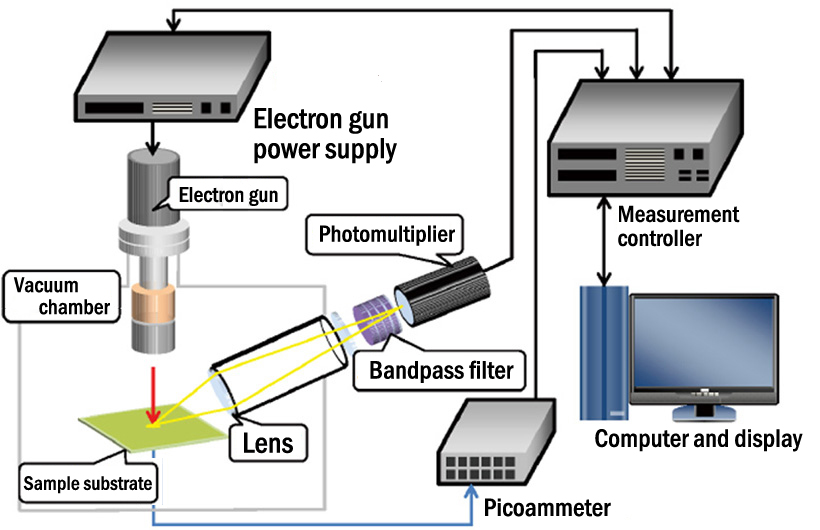
LEIPS apparatus: An electron gun, which produces electron beams, and a photodetector consisting of a lens, bandpass filter, and photomultiplier, are attached to a vacuum chamber. Various electronics, including the electron gun power supply and picoammeter, control the apparatus and collect data.


